Recently, the team of Professor Min Qiu at the School of Engineering, Westlake University, in collaboration with Dr. Kaikai Du's team at Moldnano(Hangzhou) Technology Co., Ltd, has developed a wafer-scale silicon carbide (SiC) meta-optic platform. By combining SiC diffractive optical elements (DOEs) with a metalens array, the platform separates beam splitting from individual beam focusing. The team demonstrated wafer-scale device fabrication and parallel processing of metal substrates at incident powers of several hundred watts. The study was published in PhotoniX under the title “Wafer-scale silicon carbide meta-optic platform for robust multi-beam laser processing.”

High-power laser processing is an important technology in advanced manufacturing, playing a key role in fields such as precision welding, material cutting, and additive manufacturing. The increase in laser output power provides the energy basis for multi-beam parallel processing. By splitting the beam to distribute laser energy to multiple processing positions, multi-point synchronous processing can be achieved while meeting the energy requirements of single-beam processing. Increasing the number of parallel working beams can reduce the time required for repetitive processing tasks, thereby improving processing efficiency.
Conventional multihead laser processing systems typically require separate optical components for each channel. As the number of channels increases, the systems become larger and more difficult to assemble and align. Optics for high-power precision processing must also withstand intense laser illumination while maintaining precise control over each beam’s wavefront and focusing characteristics. Combining power handling, compact integration, and individual beam control is therefore a central challenge in developing high-power parallel processing systems.
Paper: https://link.springer.com/article/10.1186/s43074-026-00294-8
A Material Platform for High-Power Beam Control
Under high-power laser illumination, optical absorption can cause localized heating and heat accumulation, affecting device performance and system operation. SiC combines high thermal conductivity, a wide bandgap, and excellent mechanical properties. Its high thermal conductivity helps dissipate heat within the device and reduces localized heat accumulation, supporting stable operation under high optical loads. Its high refractive index (n ≈ 2.6) also enables phase control through micro- and nanostructure design, providing the basis for beam splitting and focusing.
The platform uses a SiC DOE to split the incident beam and a metalens array to focus the resulting beams, as illustrated in Figure 1. A predefined phase profile in the DOE distributes the incident laser light into multiple spatial channels. After passing through a relay lens, each beam enters its corresponding metalens for wavefront shaping and focusing. Each metalens is matched to one output channel, and its phase profile can be specified independently at the design stage. This architecture allows the focusing characteristics of individual channels to be tailored to different processing requirements.
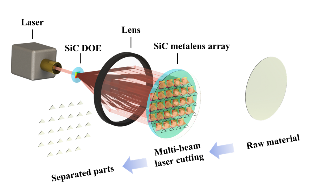
Figure 1: Optical architecture of the SiC multi-beam parallel processing platform.
From Individual Devices to Wafer-Scale Arrays
To fabricate the beam-splitting elements, the team used three successive rounds of aligned photolithography and etching to produce eight-level DOEs on a 4-inch SiC wafer. They designed and characterized 1 × 4, 1 × 9, and 1 × 26 beam-splitting configurations, as shown in Figure 2. The phase profile of each configuration was designed to distribute the incident light among the corresponding number of output channels.
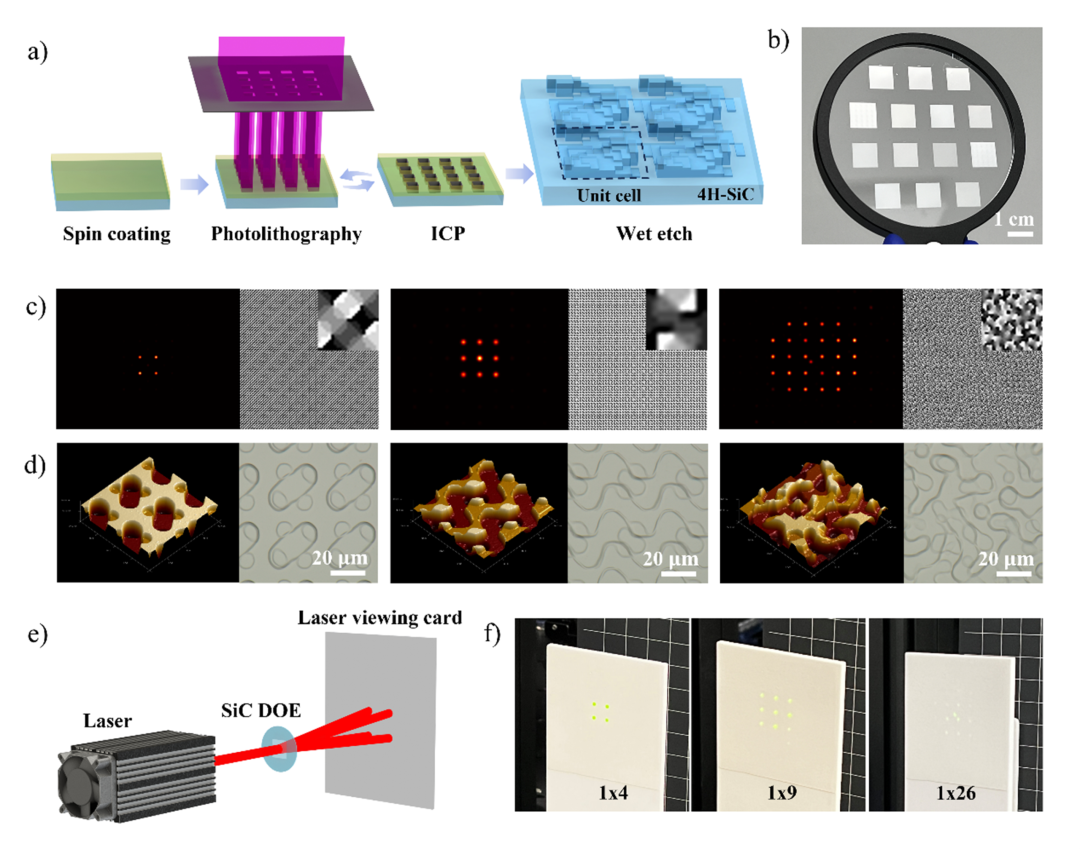
Figure 2: Fabrication and optical characterization of SiC DOEs. (a) Device fabrication process. (b) Photograph of DOE devices on a 4-inch SiC wafer. (c) Phase profiles and simulated far-field intensity distributions for the three beam-splitting configurations. (d) Atomic force microscopy and optical microscopy images of the device surface. (e) Optical setup for beam-splitting measurements. (f) Measured output spots for the 1 × 4, 1 × 9, and 1 × 26 configurations.
For the focusing elements, the team combined step-and-repeat nanoimprint lithography (S&R-NIL) with hard-mask-based pattern transfer to fabricate a SiC metalens array, as shown in Figure 3. A silicon master for a single metalens was first fabricated using electron-beam lithography and etching. The pattern was then replicated at multiple positions on a glass substrate using S&R-NIL to create a wafer-scale working mold containing 26 metalenses. The complete array pattern was subsequently imprinted into resist on a 4-inch SiC wafer and transferred into the SiC through a hard mask and etching, producing an array of nanopillar-based metalenses.
High-resolution electron-beam writing is required only to fabricate the single-metalens master. S&R-NIL is then used to produce the array working mold, which transfers the complete array pattern to the SiC wafer in a single imprint. This avoids writing every metalens individually on each wafer. Both the master and the working mold can be reused, offering a route to lower fabrication costs and consistent pattern replication for the batch production of centimeter-scale metalens arrays.
The fabricated array comprises 26 metalenses, each with a diameter of 1.15 cm and a numerical aperture of 0.5. Using critical-dimension scanning electron microscopy (CD-SEM), the team measured the diameters of eight representative nanopillar geometries on each of the 26 metalenses. The maximum measured dimensional deviation was 24.18 nm. At a wavelength of 1030 nm, the 3σ variation in focal length across the array was 10.73 μm, equivalent to just 0.11% of the design focal length. These measurements demonstrate consistency in both structural dimensions and focal length across the centimeter-scale metalens array, supporting its use for parallel focusing in multiple channels.
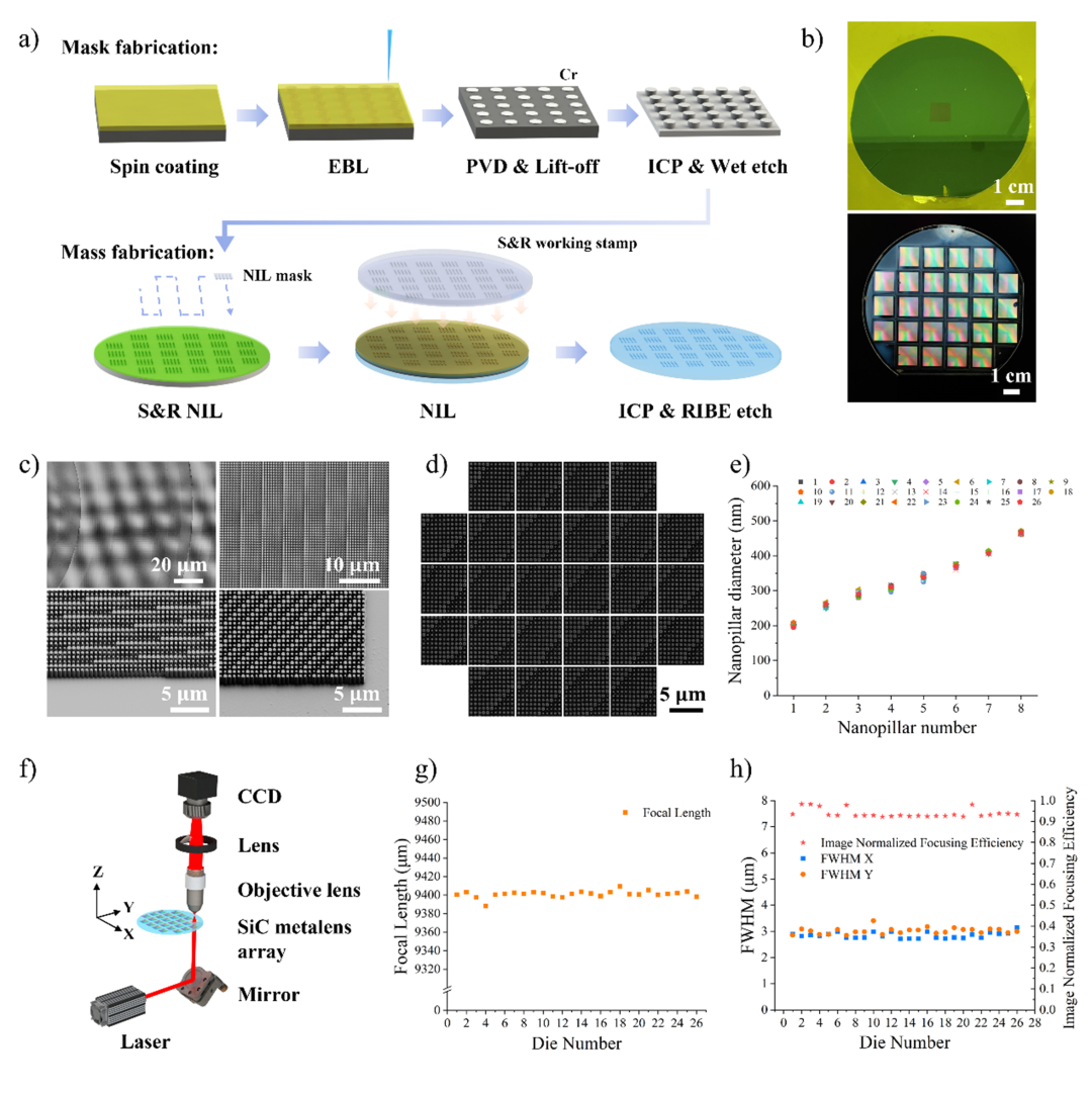
Figure 3:Wafer-scale fabrication and characterization of the SiC metalens array. (a) Master fabrication, S&R-NIL, and pattern transfer. (b) Single-metalens master (top) and 4-inch SiC metalens array (bottom). (c) SEM images of the nanopillar structures. (d) CD-SEM images acquired at corresponding locations on the 26 metalenses. (e) Measured diameters of representative nanopillar geometries across the 26 metalenses. (f) Optical characterization setup. (g) Focal length distribution across the array. (h) Focal spot full width at half maximum and image-normalized focusing efficiency.
From Optical Characterization to High-Power Metal Processing
The team evaluated the power-handling capability of the SiC DOE, which receives the full incident beam before splitting, using a high-power continuous-wave laser at 1030 nm. No visible damage was observed after 20 seconds of continuous exposure at a power density of 6.11 kW/cm². This result demonstrates the DOE’s ability to withstand high-power laser illumination under the tested conditions.
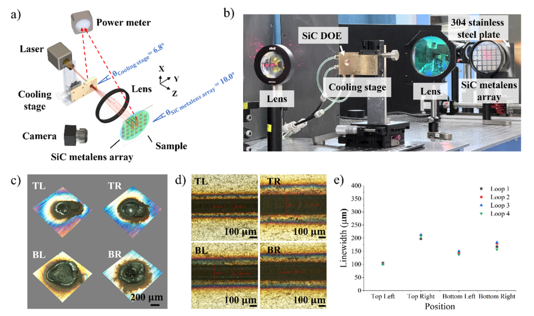
Figure 4:High-power four-beam parallel processing. (a) Optical layout of the processing system. (b) Photograph of the experimental setup. (c) Three-dimensional surface profiles of the four craters produced by parallel point processing of stainless steel. (d) Optical microscopy images of tracks produced by four-channel line scanning. (e) Track widths in each channel over four repeated scans.
The team then demonstrated four-channel parallel processing using a 1070 nm continuous-wave laser. At a total power of 732.5 W incident on the DOE, the system performed parallel point processing on 1-mm-thick 304 stainless steel. At a total DOE-incident power of 586.0 W, it performed parallel line scanning on 2-mm-thick 304 stainless steel. The results are shown in Figure 4. Repeated scanning experiments further demonstrated processing repeatability within each channel.
By combining the design and wafer-scale fabrication of SiC DOEs and metalens arrays, this study extends SiC micro- and nanophotonics from individual devices to a multi-beam processing system. Each metalens provides a phase-control element for its corresponding beam, allowing channel-specific focusing profiles to be defined at the design stage within an architecture that supports multiple channels. Further improvements in DOE fabrication precision, antireflection design, and system alignment could increase optical power utilization and improve uniformity across channels, supporting the development of compact systems for high-power parallel laser processing.
Dr. Boqu Chen, a postdoctoral researcher at Westlake University, is the first author of the paper. Professor Min Qiu of Westlake University and Dr. Kaikai Du of Moldnano (Hangzhou) Technology Co., Ltd. are the co-corresponding authors. The work was supported by the National Natural Science Foundation of China and the National Key R&D Program of China. The team also acknowledges support from the Westlake Center for Micro/Nano Fabrication and Qingdao GermanLitho Co., Ltd.