Recently, the research group led by Professor Min Qiu from School of Engineering, Westlake University developed a novel ice-assisted van der Waals metal contact technology, addressing a major challenge in perosvkite-electrode interface of halide perovskite devices. Due to the "soft lattice" nature of perovskites, traditional electrode fabrication processes easily introduce defects at the perosvkite-electrode interface, severely affecting carrier transport. The group innovatively introduced water ice as a buffer layer, which effectively protects the perovskite surface during metal deposition. Subsequently, through natural warming, the ice layer completely sublimates, enabling damage-free contact between the metal electrode and the perovskite. The performance of perovskite photodetectors fabricated based on this strategy was significantly improved: the dark current was as low as 69.7 pA at a 0.1 V bias, one order of magnitude lower than devices prepared by traditional methods; simultaneously, under 450 nm blue light excitation, the device achieved an ultra-high on/off ratio of 2.4×10⁵ and maintained a high responsivity of 42.1 A/W under low-light conditions. This research provides a new approach for developing high-performance perovskite optoelectronic devices. The related findings were published in the Cell Press journal Device under the title "Ice-assisted van der Waals Metal Contact with Halide Perovskites": https://www.cell.com/device/abstract/S2666-9986(25)00247-9.
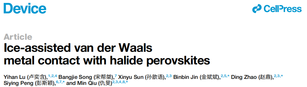
Building upon the group’s previous research of ice lithography and leveraging the excellent compatibility between water ice and perovskites, the research team developed this ice-assisted method for fabricating van der Waals contacts. The core steps include:
(1) Sample Cooling & Water Ice Deposition: Cooling the perovskite film with an attached mask to approximately 120K, and depositing a water ice buffer layer in-situ;
(2) Metal Evaporation: Depositing the metal electrode onto the ice layer;
(3) Ice Sublimation & Metal Soft Landing: Warming the sample to directly sublime the ice layer (without generating liquid water), allowing the metal electrode to soft-land on the perovskite surface, forming an atomically clean van der Waals interface. Characterization results show that the ice deposition-sublimation process does not alter the crystal structure or chemical composition of the perovskite, and there are no residual water gaps at the perovskite-electrode interface.
Taking typical inorganic perovskite CsPbBr3 as an example, the ice-assisted Au/CsPbBr3 interface is sharp with intact lattice, showing no diffusion or disordered regions. In contrast, interfaces produced by traditional direct deposition exhibit nanoscale metal atom diffusion layers accompanied by lattice disorder. Fluorescence imaging results show that after peeling off the ice-assisted deposited metal, the underlying perovskite retains high intrinsic fluorescence intensity, whereas the direct deposition method causes severe fluorescence quenching in the contact area, confirming that the ice buffer layer effectively suppresses the formation of non-radiative recombination centers. Furthermore, the team extended the ice-assisted deposition strategy to the fabrication of active metal electrodes (such as Ag, Al), further demonstrating the universality of this approach.
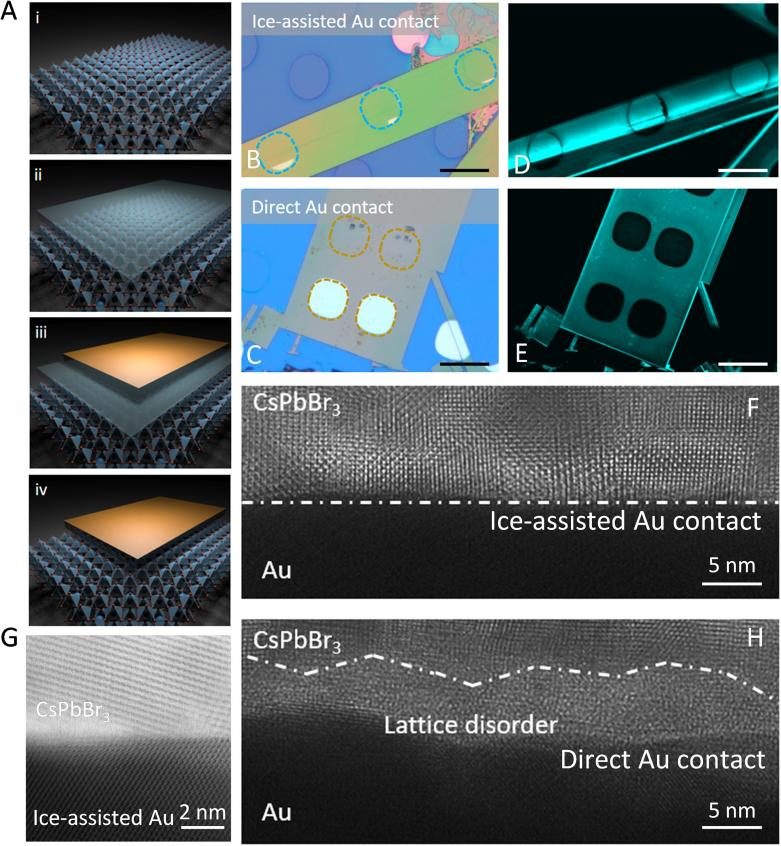
Figure 1 Schematic diagram of ice-assisted van der Waals metal contact and interface structure characterization.
Using techniques such as X-ray photoelectron spectroscopy (XPS), Kelvin probe force microscopy (KPFM), and conductive atomic force microscopy (C-AFM), the team compared the chemical states and electrical properties of the perovskite beneath ice-assisted deposited electrodes and directly deposited electrodes. The results show that the residual Au⁰ signal intensity in the ice-assisted sample is much lower than in the directly deposited sample, indicating a purely physical interaction at the interface. Furthermore, the CsPbBr3 beneath the ice-assisted contact exhibits p-type doping. C-AFM revealed uniform current distribution and higher average resistivity in the ice-assisted contact region, reducing leakage pathways caused by metal penetration. These data provide direct evidence for the "atomically clean interface" achieved by the ice-assisted strategy, supporting the observed device performance improvement.
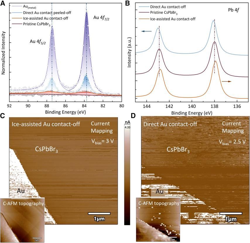
Figure 2 Chemical properties of the CsPbBr3-Au contact region based on direct metal deposition and ice-assisted metal deposition.
To evaluate the defect suppression effect of the ice-assisted strategy on perovskites, the team quantified the defect density through pulsed space-charge-limited current (pulsed-SCLC) analysis. The results show that the ice-assisted Au contact device has a lower trap-filling limit voltage, corresponding to a significantly reduced trap density. In contrast, the direct Au contact device did not achieve a transition from the trap-filled region to the trap-free region within the tested voltage range, confirming the significant suppression of lattice disorder and defects by the ice-assisted method. Additionally, carrier recombination behavior in CsPbBr3 under different contacts was characterized using micro-area time-resolved photoluminescence (TRPL) spectroscopy. This further revealed a substantial increase in the average carrier lifetime for CsPbBr3 with ice-assisted contact, effectively suppressing non-radiative recombination caused by defect states.
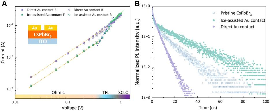
Figure 3 Surface defect state characteristics of the CsPbBr3-Au contact region based on direct metal deposition and ice-assisted metal deposition.
Ultimately, the CsPbBr3 photodetector fabricated using the ice-assisted strategy demonstrated outstanding performance: The dark current (69.7 pA @ 0.1 V) was one order of magnitude lower than that of traditional devices (0.58 nA), representing the lowest reported value for reported CsPbBr3single-crystal lateral detectors. Under 450 nm laser illumination, the device exhibited excellent photoresponse characteristics, with a low-light responsivity reaching 42.1 A/W, significantly higher than the direct Au contact device (26.9 A/W). The specific detectivity increased from 4.50×10¹² Jones to 1.39×10¹³Jones, highlighting its potential in low-light detection. The response speed of the device significantly accelerated (rise/fall times of 26.6 ms and 90.2 ms, respectively), much faster than the direct contact device (rise/fall times of 760 ms and 192.8 ms, respectively). It achieved an ultra-high on/off ratio of 2.4×10⁵ even at 0 V bias, reflecting efficient charge extraction and transport capabilities. Furthermore, in long-term stability tests, the device showed minimal photocurrent drift (only 0.02 nA/s) and extremely low dark current drift (7.78×10⁻⁴ pA/s), far superior to traditional devices which exhibited significant performance degradation. This fully demonstrates that the ice-assisted strategy can effectively suppress traps and mobile ions, enhancing device stability.
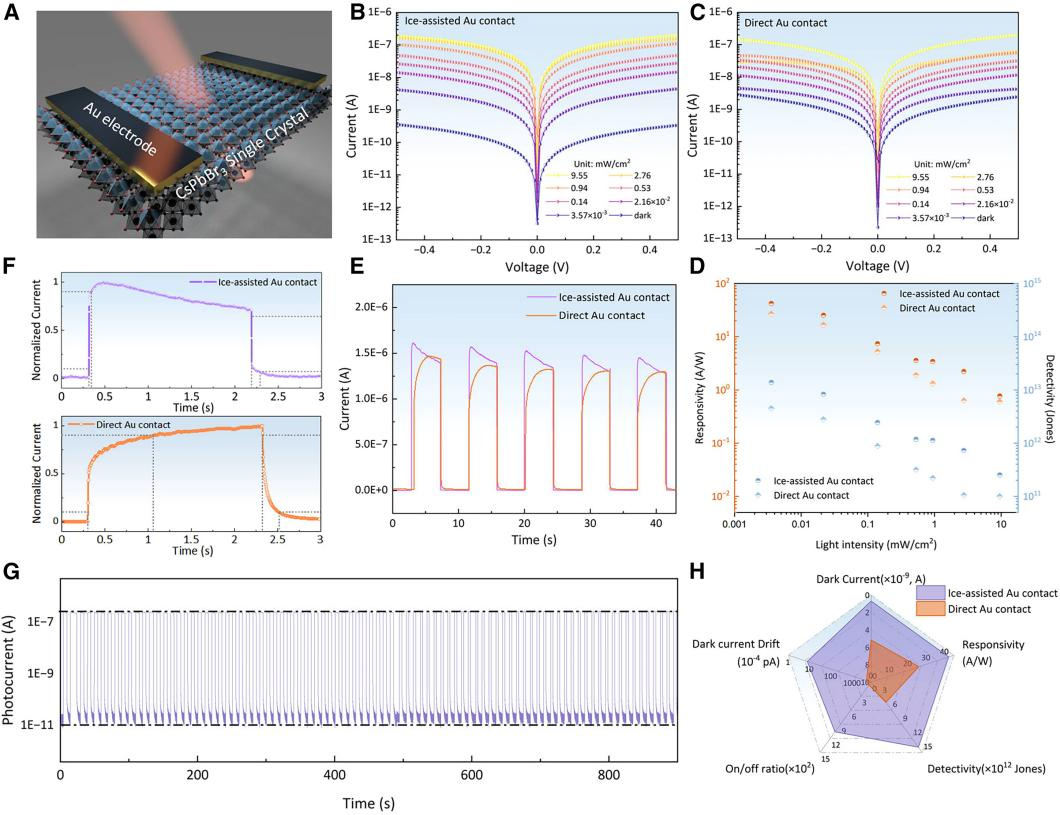
Figure 4 Performance of CsPbBr3 photodetectors based on direct metal deposition and ice-assisted metal deposition.
Highlights of this Article:
1. A solvent-free, residue-free, perovskite-compatible method for achieving van der Waals contacts.
2. An atomically clean perovskite-metal van der Waals interface.
3. Perovskite photodetectors with ultra-low dark current based on van der Waals contacts.
Yihan Lu, a PhD candidate jointly trained by Westlake University and Zhejiang University, is the first author of the paper. Professor Min Qiu and Professor Siying Peng from Westlake University, Researcher Ding Zhao from the Westlake Institute of Optoelectronics, and Dr. Binbin Jin from Hangzhou City University are the corresponding authors. This research was supported by the National Natural Science Foundation of China, the Westlake University Foundation, and the Westlake University Platforms for Material Science, Molecular Science, and Microscope and Imaging.
Source: Westlake University School of Engineering (SOE) Official WeChat Account