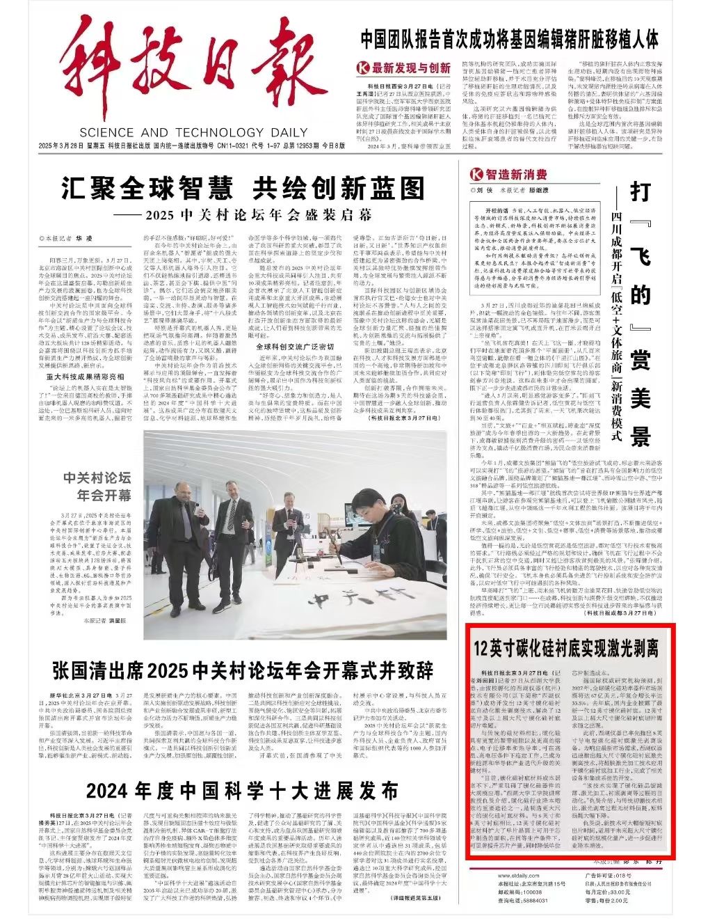
Hangzhou, China – Westlake Instruments (Hangzhou) Technology Co., Ltd., a spin-off company incubated by the Photonics And Instruments for NanoTechnology Laboratory of Westlake University, has successfully developed an automated laser lift-off (LLO) technology for 12-inch silicon carbide (SiC) substrates, overcoming the critical challenge of slicing ultra-large SiC wafers (12-inch and above). This technological milestone has been featured in authoritative media outlets including Science and Technology Daily. Below is the original report:
Science and Technology Daily, Beijing, March 27 (Reporter Yuanyuan Liu) – On March 27, Science and Technology Daily learned from Westlake University that its incubated company, Westlake Instruments (Hangzhou) Technology Co., Ltd. (hereinafter referred to as "Westlake Instruments"), has successfully developed an automated laser lift-off technology for 12-inch SiC substrates, solving the slicing challenges associated with ultra-large 12-inch and larger SiC wafers.
Compared to traditional silicon, SiC features a wider bandgap, higher melting point, superior electron mobility, and thermal conductivity, enabling stable performance under high-temperature and high-voltage conditions. These properties make SiC a key material for advancing the new energy and semiconductor industries.
"Currently, the high cost of SiC substrates severely hinders their large-scale application," explained Professor Qiu Min, Chair Professor at Westlake University's School of Engineering. "One of the most effective ways to reduce costs in the SiC industry is to manufacture larger-sized substrates. Compared to 6-inch and 8-inch wafers, 12-inch SiC substrates significantly increase the usable area for chip fabrication under the same production conditions, boosting chip yield while lowering per-unit manufacturing costs."
According to forecasts by leading international research institutions, the global SiC power device market is projected to reach $6.7 billion by 2027, with a compound annual growth rate (CAGR) of 33.5%. In late last year, domestic companies unveiled their latest-generation 12-inch SiC substrates, driving demand for slicing solutions for ultra-large 12-inch and larger wafers.
Previously, Westlake Instruments pioneered the commercialization of 8-inch conductive SiC substrate LLO equipment. In response to emerging market needs, the company rapidly developed large-format SiC substrate LLO technology, applying ultrafast laser processing to the SiC substrate industry and completing the development of related equipment and integrated systems.
"This technology automates processes such as SiC ingot thinning, laser processing, and substrate separation," said Professor Qiu. "Compared to traditional cutting methods, laser lift-off eliminates material loss, significantly reducing raw material waste."
Professor Qiu added that the new technology dramatically shortens substrate processing time and is suitable for the mass production of future ultra-large SiC substrates, further driving cost reduction and efficiency improvements in the industry.

Source: Science and Technology Daily, March 28, 2025 (Original Chinese version available upon request).

