Research background
In 1947, scientists at Bell Labs invented the world's first transistor, which triggered a revolution in microelectronics technology and profoundly changed the way of life around the world. As electronic devices become increasingly miniaturized, finding a simple, fast, and low-cost method of manufacturing micro-nano components has become a huge challenge. Although traditional direct writing manufacturing methods such as focused ion beam etching, electron beam lithography, and multiphoton polymerization still have their value in some applications, their efficiency is relatively low. Although methods such as nanoimprinting, lithography, plasma etching, and scanning laser interference etching can effectively improve processing speed, they usually require multiple processing steps, such as making masks, or need to be carried out in a very strict working environment, and often rely on special materials. In recent years, the method of using femtosecond laser-induced surface self-organized periodic structure to fabricate nanograting structures has received widespread attention. Laser-induced periodic surface structures (LIPSS) etch materials by utilizing the interference between incident light and surface electromagnetic waves, thus having high processing accuracy. Compared to traditional laser interference processing methods, the self-organized processing method has simpler experimental setups and faster manufacturing speeds.
Article Summary
LIPSS utilizes the interference between incident light and surface electromagnetic waves to etch materials, thus achieving high-precision nanofabrication. Compared to traditional laser interference processing methods, the self-organized processing method of LIPSS has simpler experimental setups and significantly faster manufacturing speeds. However, despite the enormous potential of the LIPSS method in nanofabrication, it still faces some challenges in practical applications. For example, the controllability of the LIPSS method still needs to be improved, which means that in some cases, the manufactured nanostructures may deviate from the expected design. Additionally, the specific mechanism of LIPSS structure formation, especially under different materials and conditions, still remains elusive. These complex processes involve interactions between multiple physical, chemical, and thermo-dynamic mechanisms that are not fully understood. Therefore, a lot of research and experimental work is still needed to fully realize the potential of LIPSS technology in nanofabrication.
Researchers led by Professor Qiu Min at Westlake University have extensive experience in micro-nano processing. They recently discovered that when inducing periodic grating structures on the surface of amorphous silicon thin films, the grating periodicity changes depending on the source of electromagnetic waves. Specifically, when the thickness of amorphous silicon thin films is small (50 nm) and the substrate is non-silicon material, LIPSS forms a smaller period under the dominant mode of planar waveguide and changes with the substrate material. When the thickness of amorphous silicon thin films increases to 200 nm, the dominant mode becomes the interference between incident light and quasi-cylindrical waves. Furthermore, LIPSS is induced under the combined action of near-field and far-fields. In this mode, the period of LIPSS is slightly smaller than the laser wavelength and independent of the substrate material. To validate these experimental findings, the research team also conducted numerical simulations based on finite-difference time domain (FDTD) method.
The related work was published in Issue 2 of 2023 of Frontiers of Optoelectronics under the title of "Impact of film thickness in laser-induced periodic structures on amorphous Si films".
Graphic Overview
Innovation Point: Changing the thickness of amorphous silicon thin film to induce two different periodic grating structures using femtosecond laser
The research team prepared amorphous silicon thin films with different thicknesses on multiple substrates and successfully induced an oxide periodic surface structure using a femtosecond laser pulse with a wavelength of 1030 nm (as shown in Figure 1). As shown in Figure 2, when the thickness of the amorphous silicon thin film reaches 200 nm, the period of the induced oxide grating structure is very close to the wavelength of the laser pulse. However, when the film thickness decreases to 50 nm, the period of the oxide grating decreases accordingly. It is noteworthy that changing the substrate material affects the period of the oxide grating on thinner amorphous silicon thin films but has little influence on the grating period of thicker films. Researchers speculate that the thickness of the thin film may determine the dominant electromagnetic wave mode when forming grating structures. For thinner films, due to differences in refractive index between the substrate and the thin film, planar waveguide modes become the main driving force for grating structure formation. Therefore, changes in substrate refractive index lead to changes in grating period. Especially when the refractive index of the substrate material is similar to that of amorphous silicon (e.g., when the substrate is monocrystalline silicon), grating structures will not form. For thicker films, the volume of formed oxide particles increases, and larger particles produce stronger near-field interactions. With continuous positive feedback, quasi-cylindrical waves excited by oxide particles become dominant and interfere with incident light, thereby forming oxide gratings. In this case, the grating period is independent of the substrate material.
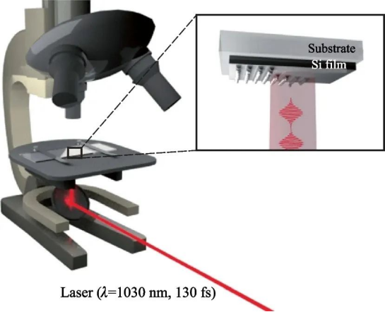
Fig. 1 Schematic diagram of laser-induced generation of periodic grating structures
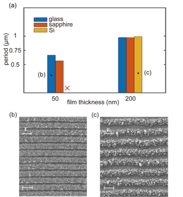
Fig. 2 (a) The relationship between the period of the periodic oxidation grating structure and the film thickness and substrate material. (b) SEM image of the periodic grating structure induced on a 50 nm amorphous silicon film on a glass substrate. (c) SEM image of the periodic grating structure induced on a 200 nm amorphous silicon film on a crystalline silicon substrate. The scale bar is 1 micron.
Innovation point 2: Verification of experimental results through numerical simulation
The research team used numerical simulation based on finite-difference time-domain method to conduct in-depth analysis of the experimental results. As can be clearly seen from Figure 3, for thinner films, the periodic energy distribution inside the film is very clear. In this case, due to the weak intensity of quasi-cylindrical waves excited by surface particles, the slab waveguide mode becomes dominant. When the substrate material is changed, the periodicity of energy distribution will also change, which is fully consistent with the experimental observation results. As shown in Figure 4, for thicker films, we can clearly see the quasi-cylindrical waves distributed in the air. Under the dominance of this mode, periodic energy distribution is formed on the interface of silicon thin film, which in turn induces the formation of periodic grating structure. In this case, the influence of substrate on the grating period becomes minimal.
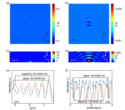
Fig. 3 Numerical simulation results of 50 nm thick amorphous silicon films on glass substrate (a,c) and monocrystalline silicon substrate (b,d), (a,b) shows the electric field distribution at the interface, (c,d) shows the side view; (e) and (f) show the statistics of the grating structural period in the simulation and experiment, respectively. The scale bar is 1 μm.
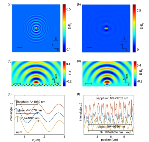
Fig. 4 Numerical simulation results of 200 nm-thick amorphous silicon films on sapphire substrates (a, c) and monocrystalline silicon substrates (b, d), where (a, b) show the electric field distribution at the interface and (c, d) are side views; (e) and (f) show the statistical results of grating structure period in simulation and experiment, respectively. The scale bar is 1 micron.
Summary and outlook
In the field of micro-nano manufacturing, laser-induced periodic surface structures (LIPSS) technology has shown great potential. By regulating the thickness of amorphous silicon films, researchers have successfully induced different periodic oxide grating structures, providing new possibilities for micro-nano manufacturing. In addition, numerical simulations based on finite-difference time-domain method provide strong verification for experimental results, further deepening the understanding of LIPSS technology. With the further development of technology and in-depth research, LIPSS technology will play a greater role in the field of micro-nano manufacturing. In order to overcome existing technical challenges, researchers need to further explore the basic principles of LIPSS, optimize experimental conditions, and improve the controllability and accuracy of structures. At the same time, the combination with other micro-nano manufacturing technologies (such as nanoimprinting, lithography, etc.) will also open up new possibilities for the application of LIPSS technology. In short, LIPSS technology has a bright future in the field of micro-nano manufacturing and is worthy of continued attention and research.
Article Link: https://link.springer.com/article/10.1007/s12200-023-00071-6
Reprinted from: Frontiers in Optoelectronics Public