01 Introduction
Professor George R. Harrison, former dean of the School of Science at MIT, once wrote in a paper that “No single tool has contributed more to the progress of modern physics than the diffraction grating.” The invention of the grating can be traced back to the late 18th century when American astronomer David Rittenhouse wrapped hair strands around a screw. Shortly thereafter, the German physicist Joseph von Fraunhofer invented the first grating ruling device. In the early years, their development was primarily driven by spectroscopists, but the applications of gratings have now long since broken through the field of spectroscopy to a wide range of applications in advanced semiconductor manufacturing, nanophotonics, and many other fields. Although the gratings have been developed over 200 years, there is still a lack of a simple, low-cost, fast, and large-area method for fabricating high-precision nano-gratings at the preparation level. Conventional nanofabrication techniques such as mechanical ruling , focused ion beam milling (FIB), electron beam lithography (EBL) , multi-photon polymerization (MPP) , laser direct writing (LDW), or thermal scanning-probe lithography (t-SPL) are inefficient. The manufacturing speeds of some other commercially available methods such as nanoimprinting, photolithography, plasma beam etching, or scanning beam interference lithography (IL) are much faster, but they are multi-step and require masks or require very demanding working environments and rely on special materials.
02 Background
To address these issues, femtosecond laser-induced self-organized periodic surface structures has gradually attracted attention in recent years for producing nanogratings. They originate from interference between the incident laser and surface electromagnetic waves (SEWs), especially the surface plasmon polaritons (SPPs). As such, it has some of the advantages of interference methods such as high precision, but laser self-organization is relatively more flexible and robust than conventional laser interference etching——capable of forming large area periodic subwavelength striped structures on almost any materials surface when under single beam large spot femtosecond laser irradiation.
However, so far, it is still difficult to achieve controlled processing of uniformly ordered nanogratings on the surface of low-loss metals such as gold, silver, and copper by laser-induced self-organization for the following reasons. Firstly, the rapid diffusion of hot electrons on the metal surface can disrupt the periodic distribution of laser energy. Secondly, long-range plasmons excited on low-loss metal surfaces are susceptible to loss of coherence due to surface defects interference during transmission. Furthermore, the debris and residual heat generated during laser ablation cause surface waves from different excitation sources to interfere with each other, resulting in disordered interference fringes.
Therefore, achieving uniform, regular, and large-area well-ordered laser-induced self-organized nanogratings is an important research direction. One of the more effective methods is to utilize the feedback effects during the periodic oxidation induced by short-range surface electromagnetic waves on thin films of high loss metals such as titanium or semiconductors such as silicon. It has the following advantages: First, the energy threshold and heat residual required for oxidation are much lower than those for ablation and does not produce large amounts of surface debris. Second, the short-range surface waves can greatly suppress the mutual interference between random defects. But its manufacturing speed is very slow, about 10-4mm2/s. And the nanograting structure based on high loss materials limits its application in fields such as plasmonic nanophotonics. In summary, it is still a challenge to solve the contradiction between manufacturing quality and efficiency of self-organized nanogratings.
03 Innovation Research——Laser-induced self-organized nanograting on the surface of metal/semiconductor composite film
Recently, researchers in Min Qiu's group in the school of Engineering at Westlake University have innovatively proposed an approach by utilizing metal and semiconductor composite film to solve the bottlenecks.
As show in Figure 1a, they have demonstrated that the rapid fabrication of wafer-level uniformly regular nanogratings can be ingeniously achieved by coating a tens of nanometers thick amorphous silicon film on the surface of a silver film, and the manufacturing speed can be increased to over 100 mm2/s by using line spot scanning.
In addition to the increased manufacturing speed, the line spot has an additional benefit of forming a straight "seed" structure at the center of the spot to enhance the quality of the self-organized nanograting. Further, they proposed to use the "artificial seed" of laser direct writing to manipulate laser-induced self-organized nanograting, which not only effectively improves the uniformity of the grating, but also further enriches the diversity of processing methods and solves the problem of a single self-organized manufacturing process.
The related research, titled “Surface plasmons interference nanogratings: wafer-scale laser direct structuring in seconds”, was published on June 23 in Light: Science & Application. The first author , Jiao Geng, and co-authors Wei Yan, Lipin Shi, Min Qiu are all from Westlake University, with Lipin Shi and Min Qiu as corresponding authors.
In this research system, metal and silicon films play different roles but both complement each other with several advantages. Firstly, it has a good antireflection effect when a certain thickness of silicon film is coated on the metal film surface. Therefore, the efficiency of laser energy utilization can be significantly improved, as shown in Figure 1b. Increased energy efficiency can in turn increase manufacturing speed. Secondly, the incident laser energy is effectively trapped in the silicon film, as shown in Figure 1c, so that the oxidation reaction-induced self-organization process is localized to the silicon film surface, thus avoiding the adverse effects caused by hot electron diffusion in the metal and so on.
Furthermore, compared with the short-range electromagnetic waves on the surface of the single-layer silicon film, the metal film can support the transmission of long-range surface plasmons, so it can effectively increase the pulse number and improve the manufacturing speed.
Finally, the dielectric nanogratings formed on the surface of the low-loss metal film have a high Q-factor, leading to excellent applications in numerous fields such as sensing and low-light nonlinear enhancement.
In short, the composite thin film system utilizes the laser-induced oxidation on the upper silicon film surface to enhance the controllability of self-organized nanostructures, while the lower metal film is used to excite long-range surface plasmons to enhance the manufacturing speed, which is greatly superior to previous self-organized nanogrdting formation processes on a single film or bulk material.
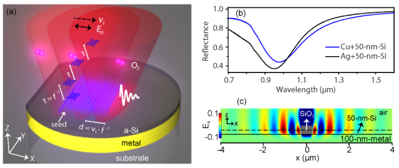
Fig. 1 (a)Scheme of femtosecond laser-induced self-organization of nanogratings on silicon-on-metal thin films. (b) Normal incidence reflection spectra of 100-nm-thick Cu and Ag coated with 50 nm of Si. (c) Cross-sectional electric field distribution in the silicon film after the formation of oxide nanoparticles, where the polarization direction of incident light along the x-direction.
More interestingly, the authors also found that the morphology of self-organized nanograting was dependent on the scanning speed. The oxidation nanograting is formed under slow scanning speed, as shown in Fig. 2a, d, while the ablative nanograting is formed under fast scanning speed, as shown in Fig. 2e, f. However, the team achieved the fastest manufacturing speed ever recorded for both oxidation and ablation-dominated nanogratings, as shown in Fig. 2c, h, with a periodic error of <0.5%, as shown in Fig. 2b, g.
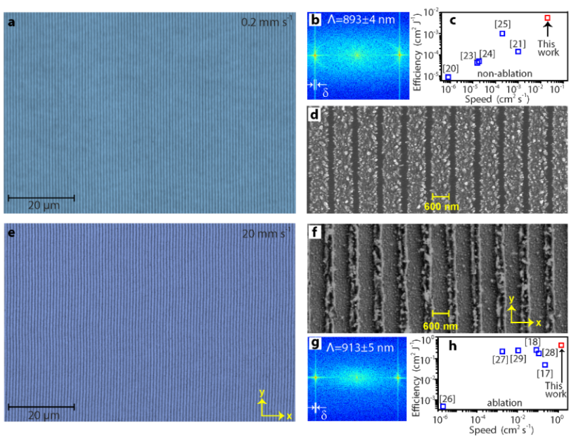
Figure 2. Optical microscopy (a) and scanning electron microscopy (d) morphologies of the oxidation nanogratings and the corresponding Fourier transform (b). Optical microscopy (e) and scanning electron microscopy (f) images of the ablative nanograting and the corresponding Fourier transform (g). The manufacturing speed and the energy utilization efficiency of the nanograting based on the oxidation reaction (c) and ablation effect (h) in this paper compared with those in the literature.
For this new physical discovery, the authors constructed a detailed mathematical model, as shown in Figure 3. It was found that during the slow scanning speed, the accumulated pulse number is higher and the silicon film surface is fully oxidized, forming a higher ablation threshold of SiO2 than that of silicon thus suppressing the ablation effect. However, under the fast scanning speed, the silicon film surface is not sufficiently oxidized, so the ablation effect dominates, but the periodic material distribution formed by the pre-oxidation process effectively enhances the quality of the ablation grating. Therefore, regardless of whether the oxidation reaction or the ablation effect dominates, the formed nanogratings have very regular structures and uniform periods.
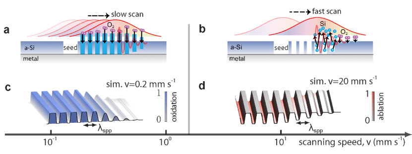
Figure 3. Physical model of oxidation and ablative nanograting formation (a, b) with theoretical calculation results (c, d).
This work is expected to build a bridge between ultrafast laser micro/nano fabrication and nano-photonics. The authors demonstrate the application of metal-surfaced dielectric nanogratings in refractive index sensing, as shown in Figure 4. The Q-factor exceeds 40, and the corresponding refractive index sensing sensitivity exceeds 700 nm/RIU. In the past, sensor chips based on conventional micro/nano fabrication processes are generally capable of manufacturing only small sensing areas, while the laser-induced self-organization method can easily process wafer-scale size high-sensitivity sensing chips, as shown in Fig. 4e, and thus offers great advantages in practical applications.
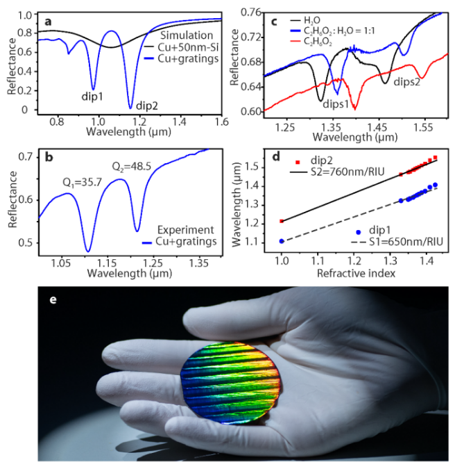
Figure 4. Numerical simulated (a) and experimental measured (b) reflection spectrum of a silicon oxide nanogratings formed on a copper film coated with a 50 nm silicon film in air, as well as the reflection spectrum in different liquid environments (c). Measured spectra dips versus refractive index of the involved liquids. (d) Rainbow-colored photograph of a 2-inch wafer with nanogratings (e).
Professor Gunter Steinmeyer of the Max Bonn Institute and Humboldt University wrote a commentary on the paper entitled "Creating the perfect plasmonic wave".
Paper Link:
https://doi.org/10.1038/s41377-022-00883-9
https://doi.org/10.1038/s41377-022-00926-1
Paper Information
The paper titled “Surface plasmons interference nanogratings: wafer-scale laser direct structuring in seconds”published in Light: Science & Applications.
Reprinted from: LightScienceApplications