When walking into the Nanophotonics and Instrument Technology Laboratory located in Building 2, Yunqi Campus, there are lots of people working in the clean room, which maintains a very low concentration of airborne particulates. As the name implies, The laboratory is mainly employed for exploring the interaction between light and nanoscale structures and materials, and developing functional optoelectronic devices or flexible manufacture processes. One of the key directions is called “ice lithography”, which is a novel attempt including using water ice and electron beam to achieve nanofabrication. The results have been reported in Nano Letters, Nanoscale, Applied Surface Science and other journals. All processes are based on the self-built dedicated equipment named “Ice Lithography 2.0".
What is Ice Lithography?
At the very beginning, let’s consider how to write the words "Happy Birthday" on the cream cake with chocolate powder. It contains three steps: Firstly, you could put a plastic mold with letter-shaped gaps beyond the cake. Secondly, the chocolate powder is sprinkled through the mold. And finally, the mold is removed and the words "Happy Birthday" appears. And it has similar steps for most lithographic nanofabrication approaches, like electron beam lithography.
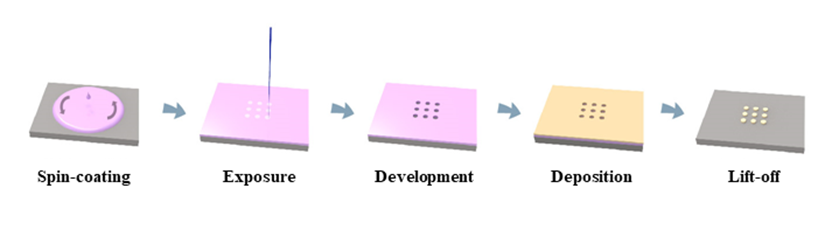
Key steps in common EBL process
Figure above shows the critical processes about electron beam lithography. The resist, which is sensitive to electrons, needs to be coated on a silicon wafer. Then the programmed e-beam irradiates specific area. Resist property in exposed area will changed and dissolved by organic solvents. And metal film is deposited on the resist mask. Finally, the resist could be removed by organic solvents and the metal structure will remain.
Common EBL process has been widely employed in laboratory. Yet the resists limit its application. “The process of spin-coating is like spreading an egg cake on plate. If the plate is unflat or relatively small, the cake will not spread evenly. Besides, the material of the plate could not be fragile; otherwise the cake will easily break.” said Zhao Ding, a vice researcher in Qiu Min's laboratory.
These problems could be avoided when using water ice as resists. In this case, the ice layer is from condensed water vapor at 140 K in the vacuum chamber.
“In ice lithography system, the sample is cooled down before water vapor injection, which will condense into a thin ice layer.” Zhao Ding said that the shortcomings of common resists are precisely the advantages of ice resists. "The ice film could cover any shape of the sample surface, even the smallest sample. Besides, ice lithography has no needs for spin-coating or baking, which may damage fragile substrate.”
Additionally, according to the special properties of water ice, the fabrication process can be greatly simplified. "When the electron beam incident the ice layer, the ice will 'disappear' since the electrons ionize and decompose the water molecules. As the results, the e-beam could construct the ice structure without development, which avoids the pollution and unexpected resist residue, " Zhao Ding explained. The extra ice layer will sublimate when the temperature of the sample rises after metal deposition, as if it never existed. For comparison, common resists demand specific solution to lift-off.

Key steps of ice-assisted electron beam lithography
Ice Lithography 2.0: “Wafer in, Device out”
In 2012, shortly after Qiu Min returned to teach at the Royal Swedish Institute of Technology, he started the "Ice Lithography" project. After six years of hard work, he and his team develop the first ice lithography system in China. When comes to Westlake University, Qiu Min, with the support of the National Natural Science Foundation of China's major scientific research instrument development project (free application category), has devoted himself to the research and development of "Ice lithography System 2.0" with more powerful functions. They dedicated to simply the processing in electron beam lithography and create the all-in-vacuum nanofabrication system, which including ice condensing, e-beam exposure and metal deposition.
Qiu’s team attempts to explore more possibilities in ice e-beam lithography. For example, They found using appropriate parameters, the e-beam could image the sample without breaking ice resist. As the result, the characteristics of the sample provide a precise reference for exposure, which is called “in-situ alignment”. It is critical to simply nanofabrication processes, especially for 3D multilayer structure.

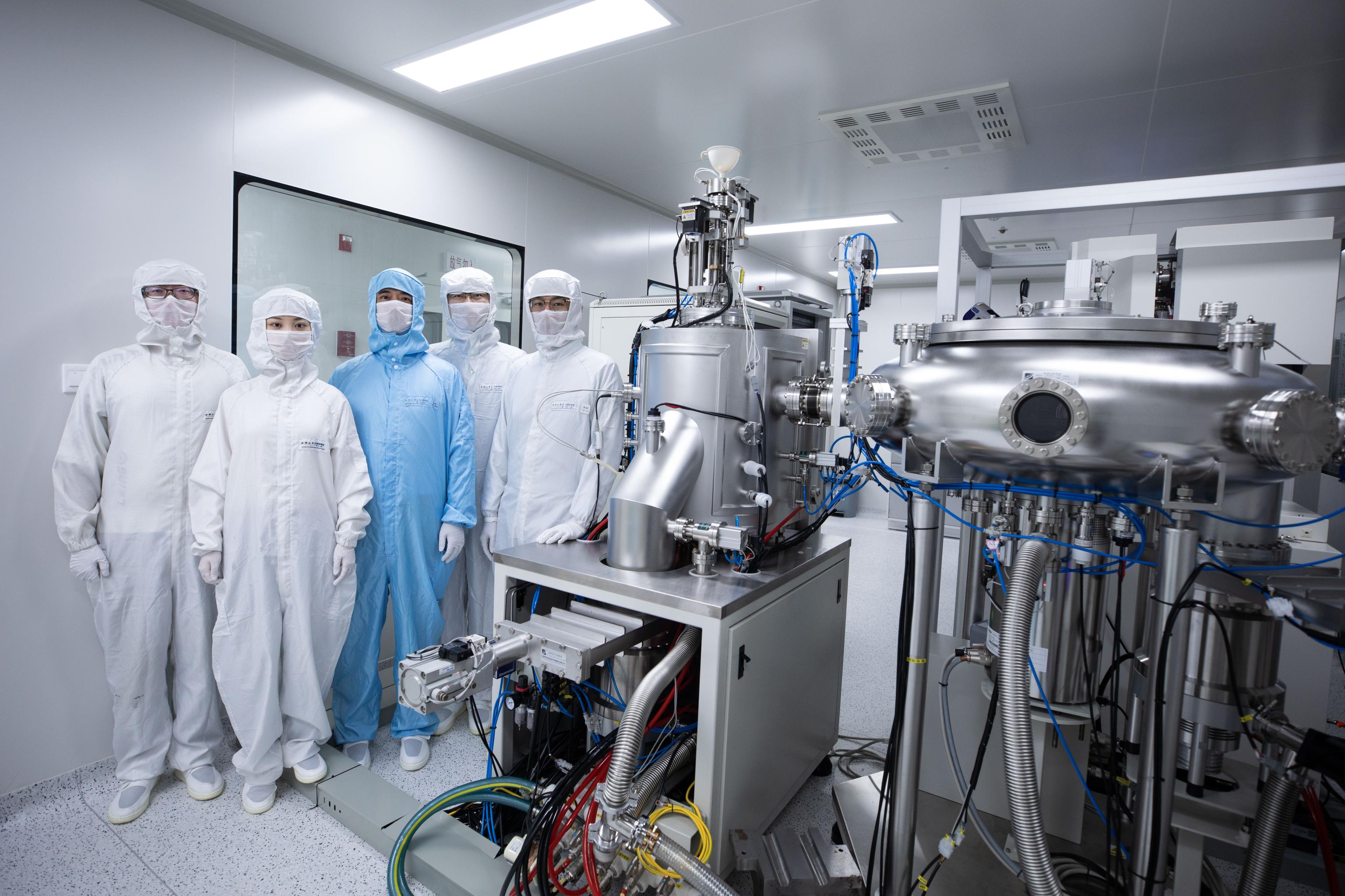
Photography of “Ice Lithography 2.0” system
Wu Shan, a PhD student in Qiu Min's lab, found a way to control the depth of ice pattern. She found that the thickness of the removed ice layer is linearly related to the amount of electrons, which is different with most common e-beam resist. As the result, the depth of the remained ice could be easily controlled by setting calculated parameters.
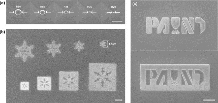
Pattern on 300nm ice layer, The scale bar is 1μm.
Hong Yu and other team members found an easy way to strip the unexpected film from the sample surface. When ice layer sublimated in vacuum, Film deposited on ice will be broken and split into many pieces. As the result, nitrogen flow could remove them directly. Compare with common EBL, Ice lithography has no needs for any liquid. And it is important for fabricating some solvent-sensitive material. Besides, they achieved nanostructure based on the fiber end face, which is hard to spin-coating.
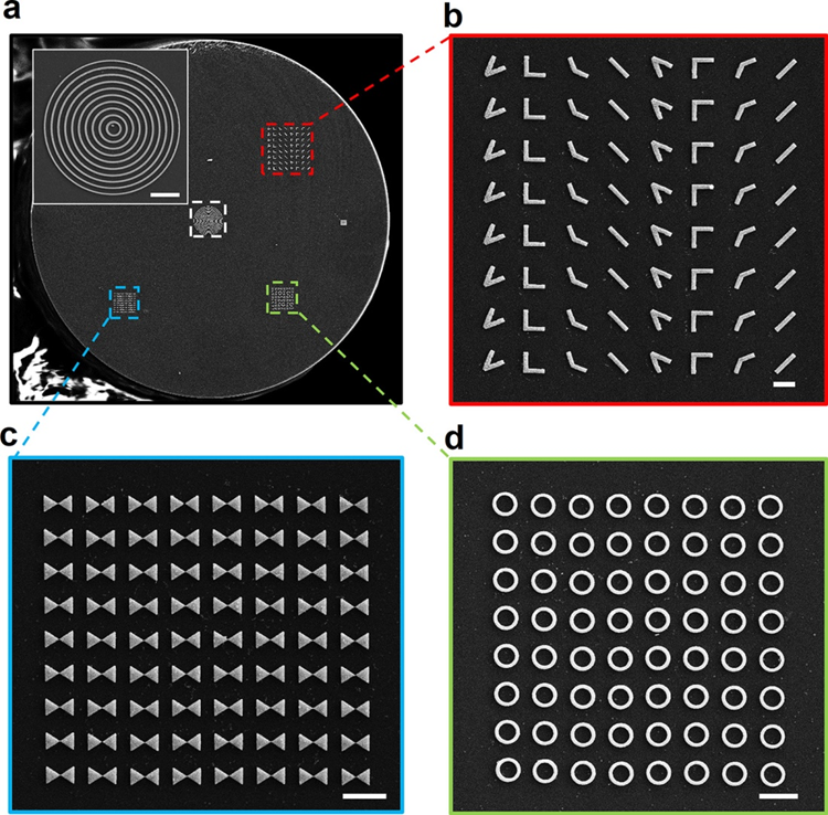
Nanostructures fabrication on fiber end faces using ice lithography
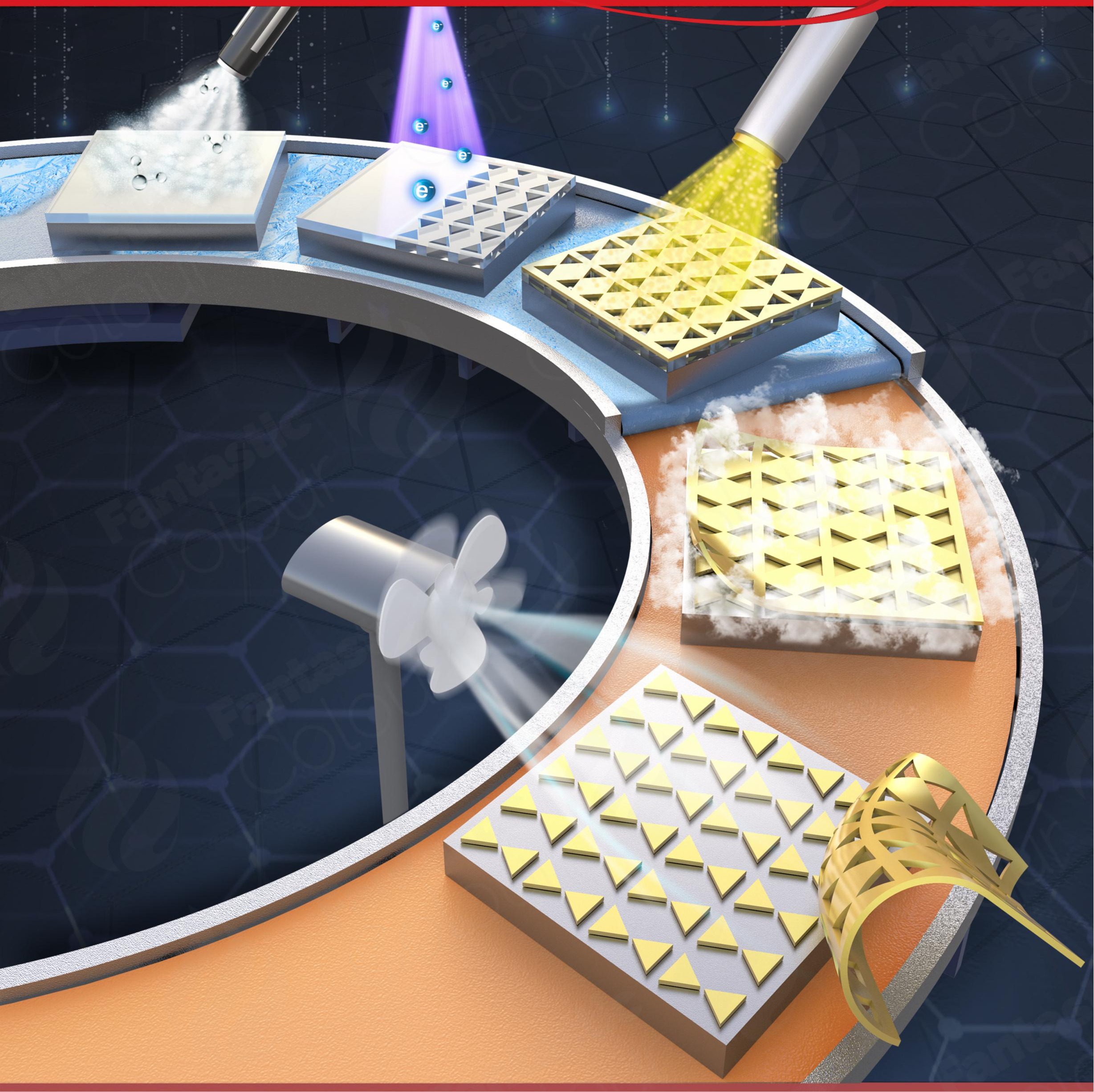
Schematic of solvent-free fabrication
In addition, based on the interaction between ice and electrons, "we could create pattern on the monolayer two-dimensional material directly, and produce peculiar properties of materials by artificial construction." Yao Guangnan, a PhD student in Qiu Min's lab, is currently conducting this research.
"Wafer in, device out." Four short words depict their ambitious goal for Ice lithography: the material is sent to the system, and then the device will be taken out.
Qiu Min said, ice lithography still belongs to electron beam lithography. However, as a green and "gentle" approach, it is especially suitable for non-planar substrates or fragile materials, and even biological materials. Professor Lei Zhou, head of the Department of Physics at Fudan University and an expert in metamaterials and metasurface, consider that the ice lithography is of great importance for the development of integrated and functional optoelectronic devices. "Ice lithography could flexibly combine the optical frontier of metasurfaces with the widely used optical fibers, which providing a suitable platform for the former and giving a new lease of life to the latter." He said.
Painful and joyful lonely dancers
Qiu Min's team has been studing in the field of ice lithography for eight years. Initially, he found that a research team at Harvard University had demonstrated a prototype of "ice lithography" for the life sciences, which inspired him to see the great potential of this technology in the field of micro and nano processing. With the power of his dream, Qiu Min inspired Zhao Ding, one of the first PhD students he recruited after returning to China, and they decided to take on the challenge together. "Instead of being a follower on a well-traveled path, I think it is the choice most researchers prefer to make to break a new path." Zhao Ding said.
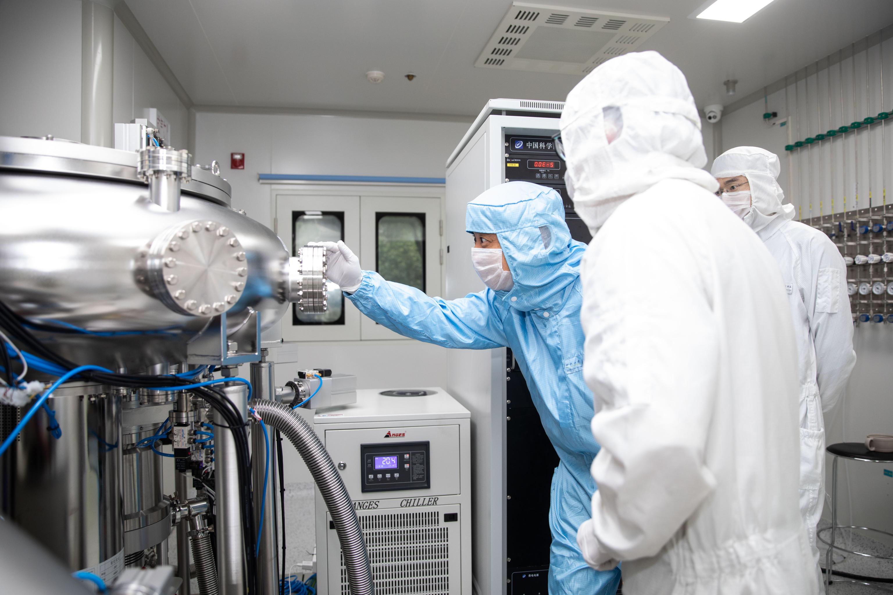
Qiu Min and team members are testing Ice Lithography System 2.0
At the end of the latest article published by Qiu Min's team, they expect the future of ice lithography. There is no doubt that ice lithography will focus on overcoming the limits of traditional lithographic methods. Benefit from the biocompatibility of water, it is expected that the manufacture of photonic waveguides or electronic circuits on biological samples will be possible. And it will unprecedentedly increase the ability to construct biological samples artificially, while opening up entirely new interdisciplinary directions.
A butterfly in South America flaps its wings and triggers a hurricane in the Atlantic Ocean. Who says there is no such possibility?
Group photo of some members of Qiu Min's team
Relative articles:
[1] Direct electron-beam patterning of monolayer MoS2 with ice
https://doi.org/10.1039/D0NR05948J
[2] Lithographic properties of amorphous solid water upon exposure to electrons
https://doi.org/10.1016/j.apsusc.2020.148265
[3] Solvent-Free Nanofabrication Based on Ice-Assisted Electron-Beam Lithography
https://doi.org/10.1021/acs.nanolett.0c03809
Reprinted from: Westlake University