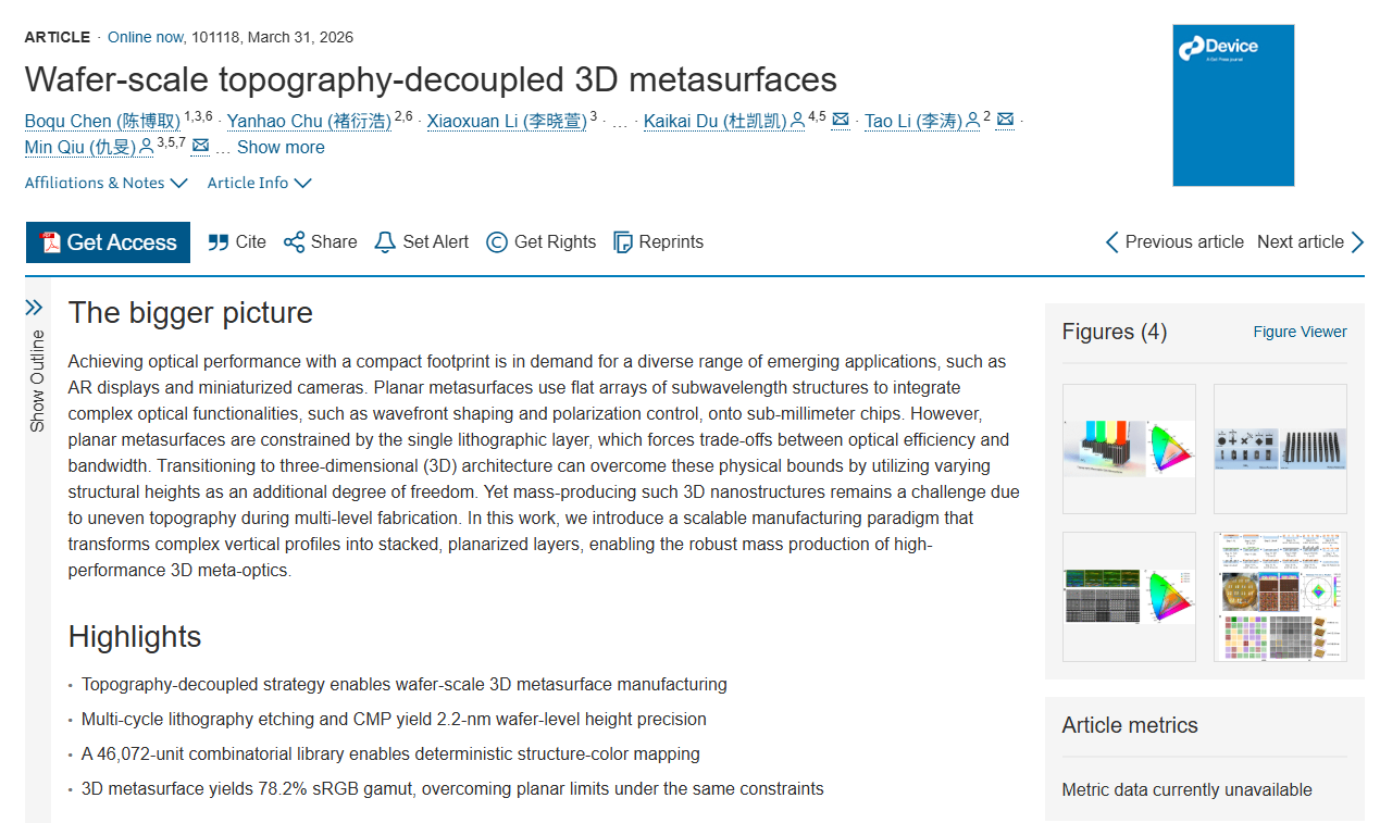
Recently, Professor Min Qiu’s research team achieved a significant breakthrough in the field of three-dimensional metasurface manufacturing. The research paper titled “Wafer-scale topography-decoupled 3D metasurfaces” authored by PhD student Chen Boqu (Class of 2021), has been accepted by the journal Device. This study presents a wafer-scale topography-decoupled manufacturing strategy for 3D metasurfaces, providing a new route toward the large-area, high-precision, and scalable fabrication of high-performance 3D metasurfaces.
Metasurface devices manipulate light through artificial structures at the subwavelength scale and have shown broad potential in integrated photonics, display technologies, and imaging systems. However, conventional planar metasurfaces are fundamentally constrained by the geometric degrees of freedom available within a single structural layer. As a result, phase control, spectral response, and resonance strength are often intrinsically coupled, which limits the achievable performance of such devices. Although the introduction of three-dimensional architectures offers a promising route to overcome these limitations, existing technologies have long been restricted by fabrication efficiency, insufficient vertical height precision, and the accumulation of surface topography during multilevel processing.
To address this challenge, the team developed a topography-decoupled manufacturing concept by integrating chemical mechanical polishing with multi-cycle overlay lithography and etching. This approach transforms the construction of complex vertical topographies into a sequence of planarized two-dimensional processing steps, thereby enabling independent control over in-plane geometry and vertical height. This strategy overcomes the difficulty of scaling conventional 3D nanostructure fabrication to large areas due to accumulated surface topography, and establishes a new process foundation for 3D metasurface manufacturing compatible with standard semiconductor technologies.
This work provides a new methodological foundation for the high-precision and scalable fabrication of 3D metasurfaces, while also offering process support for the development of structural-color displays, meta-optical devices, and next-generation integrated nanophotonic systems. The publication of this study further extends the manufacturing pathway of metasurfaces from planar structures to three-dimensional architectures, and provides new insight into the practical realization of high-performance nanophotonic devices.
Paper Linking:https://www.cell.com/device/abstract/S2666-9986(26)00070-0