Recently, Professor Min Qiu's research team has made a breakthrough in the field of ultra-precision laser processing of silicon carbide (SiC). The research results of the 2021 doctoral student Xiaoyu Sun, "Controlled Growth of Multifilament Structures with Deep Subwavelength Features in SiC via Ultrafast Laser Processing", have been successfully accepted by the journal Photonics. The team utilized ultrafast laser technology to successfully fabricate ultra-highly uniform nanoscale stripe structures with an aspect ratio exceeding 3200:1 within SiC crystals. This achievement is expected to provide technical references for the manufacturing of next-generation quantum devices and photonic chips.
The research team innovatively used elliptical Gaussian beams instead of traditional circular beams and precisely controlled the pulse duration (optimized to 10 ps) to effectively suppress the randomness in the multi-filament formation process, achieving highly ordered parallel multi-filament structures. Under the optimal processing conditions, the fabricated nanoscale stripe structures can reach a length of 90 micrometers, with the minimum line width being only 28 nanometers (approximately 1/34 of the laser wavelength), setting a record for processing deep subwavelength feature structures within transparent crystals.
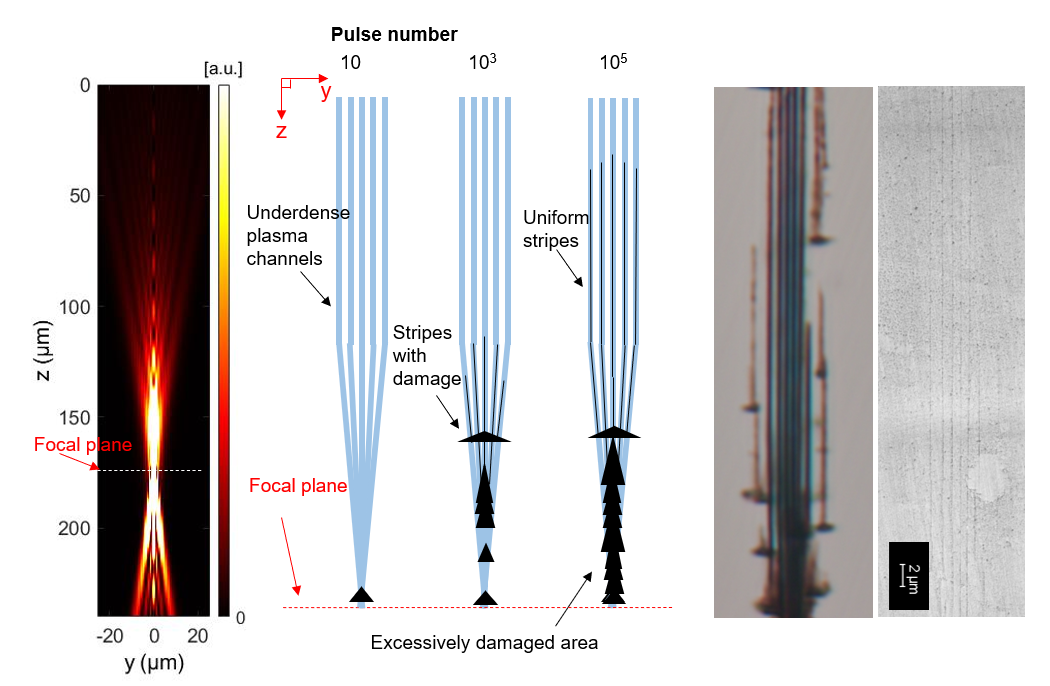
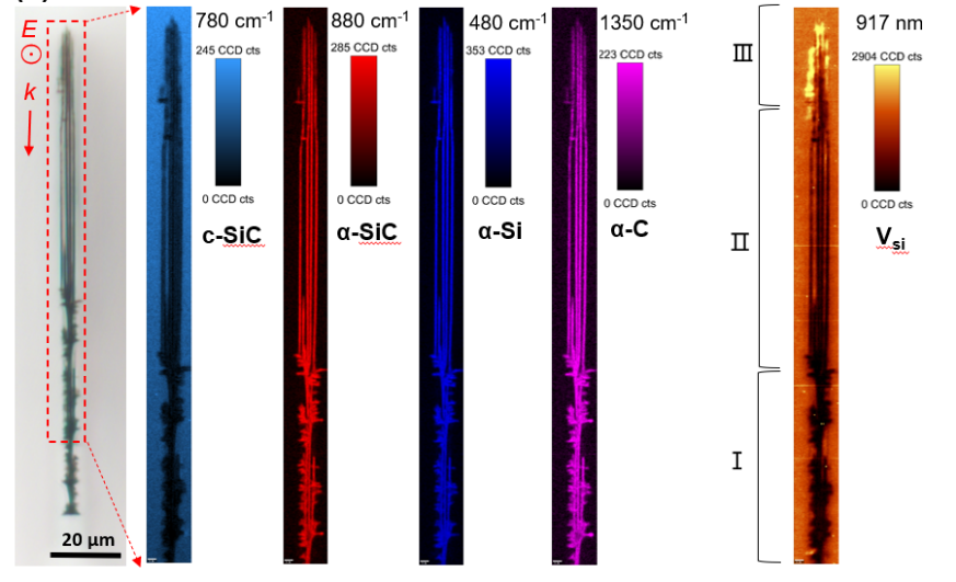
Characterization analysis indicates that the modified region transforms from single-crystal silicon carbide to amorphous silicon carbide and can further decompose into silicon and carbon. More significantly, silicon vacancy color centers can be successfully induced in the area with lower laser power density, which may provide a new technical reference for the application of SiC in the field of quantum luminescence.
This research not only demonstrates the great potential of the laser multi-beam effect in nanofabrication, but also provides new ideas for the manufacturing of three-dimensional integrated photonic devices. It demonstrates that by ingeniously regulating the nonlinear interaction between laser and matter, the diffraction limit and planar processing constraints of traditional lithography technology can be overcome, opening up a revolutionary technical path for realizing the next-generation multifunctional, high-density integrated "lab-on-a-chip" system.
Paper Link:https://www.mdpi.com/2304-6732/12/10/973