Cryogenic Electron-Beam Writing for Perovskite Metasurface
Research background
Research into perovskite materials originated in the early 20th century, but it was not until 2012 that perovskite solar cells (PSCs) broke through the 10% efficiency barrier, drawing global attention to their vast potential applications in the photovoltaic field. Over the past decade, the efficiency of PSCs has soared to over 25%. In the modern optoelectronics arena, the exceptional photovoltaic properties of perovskite materials, such as high-efficiency light absorption, long carrier diffusion lengths, and lifetimes, have led to their widespread use in various device domains including LEDs, photodetectors, and lasers. Currently, research on perovskite materials and their optoelectronic devices has taken a commanding height in the global competition for photovoltaic energy, garnering extensive attention from both the academic and industrial sectors.
Tremendous effects, such as compositional and defect engineering, have been made to improve the intrinsic photoelectric properties of halide perovskites (HPs). To break through the exiting material limitations, metasurface is introduced as a building block to achieve unprecedented optical response and magic light control functionalities. However, nanopatterning on HPs is challenging as they are readily destructured by the organic solvents in standard lithographic processes.
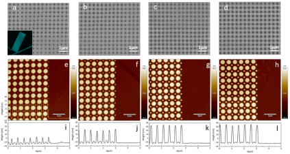
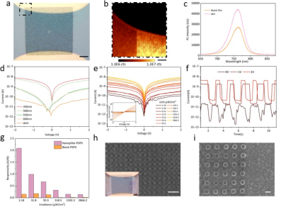
In recent times, Professor Min Qiu’s research team has achieved a breakthrough in the field of perovskite micro-nano fabrication. They have proposed a simple and efficient cryogenic electron-beam direct writing method. Compared to traditional electron-beam exposure procedures, this method not only enables non-destructive preparation of high-precision perovskite-based metasurfaces (with minimum pattern sizes as small as 70 nm), but also utilizes the enhanced absorption effect of metasurface structures. As a result, the responsivity of perovskite-based photodetectors has been increased by a factor of 15. Additionally, the material’s stability has been simultaneously enhanced through a self-encapsulation effect.

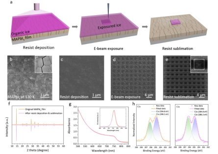
Schematic of the article
The research findings, titled ‘Cryogenic Electron-Beam Writing for Perovskite Metasurface,’ have been successfully published in the journal Nano Letters. Dr. Binbin Jin, former assistant researcher at the Photonics and Instrumentation for Nanotechnology Laboratory of Westlake University, and doctoral student Yihan Lu from the class of 2021 are co-first authors of the article, while Researcher Ding Zhao and Professor Min Qiu serve as corresponding authors

Screenshots of the paper
Technical Highlights
Fully non-destructive and flexible HP-based metasurface fabrication.
The use of solid anisole ice resist plays a crucial role in our strategy. The unique properties of solid anisole ice allow us to eliminate the issues of chemical residue and degradation caused by polar solvents and resists in conventional EBL process. Meanwhile, it maintains flexible e-beam patterning capabilities, enabling fabrication of arbitrary HP-based metasurface without surface destruction. This modified EBL strategy, as a fully protective nanofabrication platform, demonstrates unparalleled compatibility with perovskite materials. We anticipate that this approach could further promote novel optoelectronic functionalities of HPs that are inaccessible without metasurface and revolutionize device performance.

Simultaneous patterning and self-encapsulation.
By controlling the exposure voltage, a thin film of cross-linked resist could be naturally induced onto HPs, isolating devices from oxygen and moisture continuously during operation. The simultaneous patterning and self-encapsulation process could enhance stability of the perovskite films and the long-term stability of the devices, which significantly increases its potentials for future industrialization.

Efficient perovskite photodetector performance.
As a proof of concept, we designed and sustained near-perfect absorption nanopillar metasurfaces on perovskite. With the absorption-enhanced nanopillar metasurfaces, our perovskite photodetector exhibits 14 times enhancement of responsivity and excellent stability, compared with the unadorned one. The creation of such improvement with exposed exposed anisole nanostructures not only highlights the feasibility of OIL for achieving functionalized HPs metarufaces, but also paves the way for their application in high-Q microlasers, nonlinear nanophotonics, and multiresonant optics.

We believe that this manuscript meets the outstanding standards of Nano Letters and would like to thank you for considering it.
Article Links: https://doi.org/10.1021/acs.nanolett.4c00954

